Scavenging browsing Mobile
Hot Search: SSM3K35MFV SSM3J36MFV 2SK3376TT-B
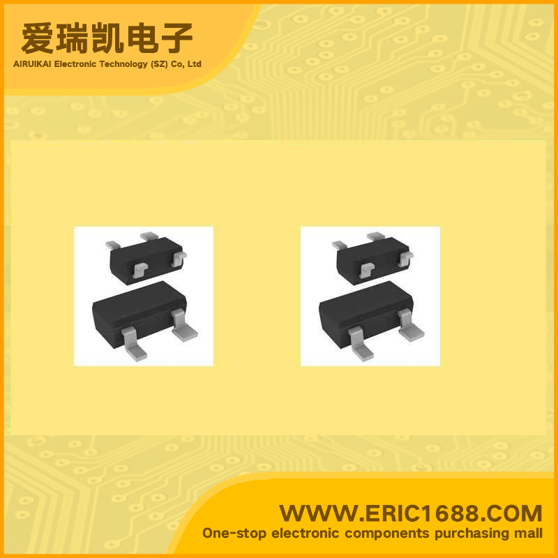
BF998R MOSFET N-Channel 12V 30mA SOT-143 marking MOP no secondary breakdown/fast switch/high input impedance
最大源漏极电压Vds Drain-Source Voltage | 12V |
最大栅源极电压Vgs(±) Gate-Source Voltage | |
最大漏极电流Id Drain Current | 30mA |
源漏极导通电阻ΩRds DΩ/Ohmain-SouΩ/Ohmce On-State Ω/Ohmesistance | |
开启电压Vgs(th) Gate-Source Threshold Voltage | 2V |
耗散功率Pd Power Dissipation | 200mW/0.2W |
Description & Applications | Silicon N-channel dual-gate MOS-FETs VHF and UHF applications with 12 V supply voltage, such as television tuners and professional communications equipment. FEATURES • Short channel transistor with high forward transfer admittance to input capacitance ratio • Low noise gain controlled amplifier up to 1 GHz. APPLICATIONS • VHF and UHF applications with 12 V supply voltage,such as television tuners and professional communications equipment. DESCRIPTION Depletion type field effect transistor in a plastic microminiature SOT143 or SOT143R package with source and substrate interconnected. The transistors are protected against excessive input voltage surges by integrated diodes between gates and source. |
描述与应用 | 硅N沟道双栅MOS场效应管 VHF和UHF的应用程序具有12伏电压的电源电压, 诸如电视调谐器和专业的通信设备。 特点 •短沟道晶体管输入电容比具有较高的正向传输导纳 •低噪声增益控制放大器高达1 GHz。 应用 •VHF和UHF应用具有12伏电压的电源电压,如电视调谐器和专业的通信设备。 说明 耗尽型场效应晶体管在一个塑料超小型SOT143封装SOT143R相互连接的源和衬底。晶体管保护,以防止过高的输入电压浪涌门和源之间的集成二极管。 |